Home » Link Gulf – Main Store Page » Scanning Electron Microscopy
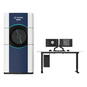
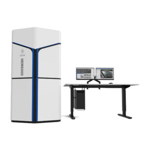
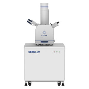
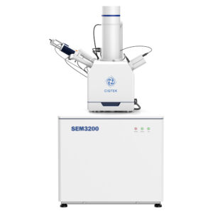
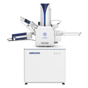
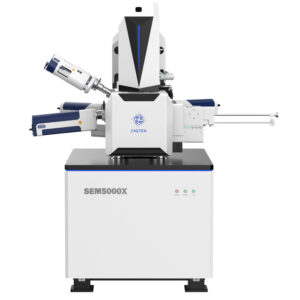
Scanning Electron Microscopy (SEM) is widely used across various fields to produce unprecedented images of the microscopic and nano-metric world.
Our Ciqtek Global family of SEM models are used in research fields and industry applications such as semiconductor, flat-panel display, and nanotechnology labs. Quality control of electronics circuits and semiconductor parts. Observation of micro-structure of Secondary cell, CNT (Carbon Nano Tube), Solar Cell, Wafer, Bonding Wire, LED and Nano technologies.
Showing all 10 results
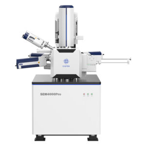
Request a Quote
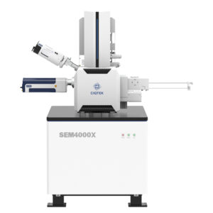
Request a Quote
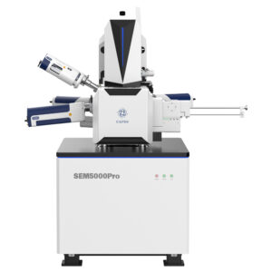
Request a Quote
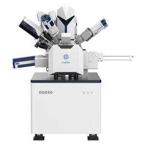
Request a Quote
Request a Quote
Request a Quote
Request a Quote
Request a Quote
Request a Quote
Request a Quote