Home » Link Gulf – Main Store Page » Scanning Electron Microscopy » in-situ MEMS-TEM-STM Multi-Field Measurement System
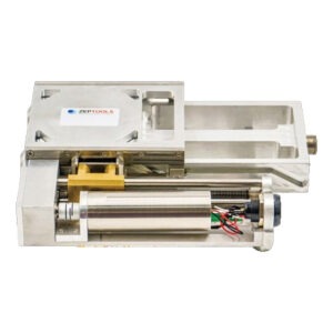
PicoFemto in-situ MEMS-TEM-STM Multi-Field Measurement System, which is an in-situ transmission electron microscope experimental system, enables researchers to construct a controlled multi-field environment (including force, heat, light, electricity, etc.) in a transmission electron microscope, to achieve in-situ characterisation of samples, such as materials or devices, under multiple excitations.
STM Multi-Field Measurement – Performance Indicators
Request a Quote
Prices shown are for the United Arab Emirates only and exclude VAT @ 5% Local Rate (Unless Otherwise Stated).
Other countries may incur additional import duties.
Please Contact Us for further details and pricing for your country or location.
PicoFemto in-situ MEMS-TEM-STM Multi-Field Measurement System, which is an in-situ transmission electron microscope experimental system, enables researchers to construct a controlled multi-field environment (including force, heat, light, electricity, etc.) in a transmission electron microscope, to achieve in-situ characterisation of samples, such as materials or devices, under multiple excitations.
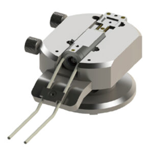
Application Scenarios: By simply changing the type of MEMS chip and applying up to four excitations to the samples with different STM probes, it can realise a variety of complex test functions and complete previously unattainable research.
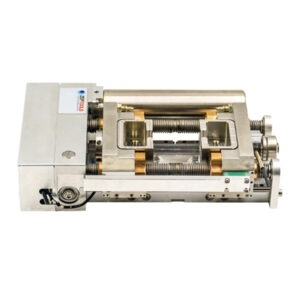
Easily obtain high-resolution images in large-scale motion, suitable for a wider range of application scenarios and sample systems.
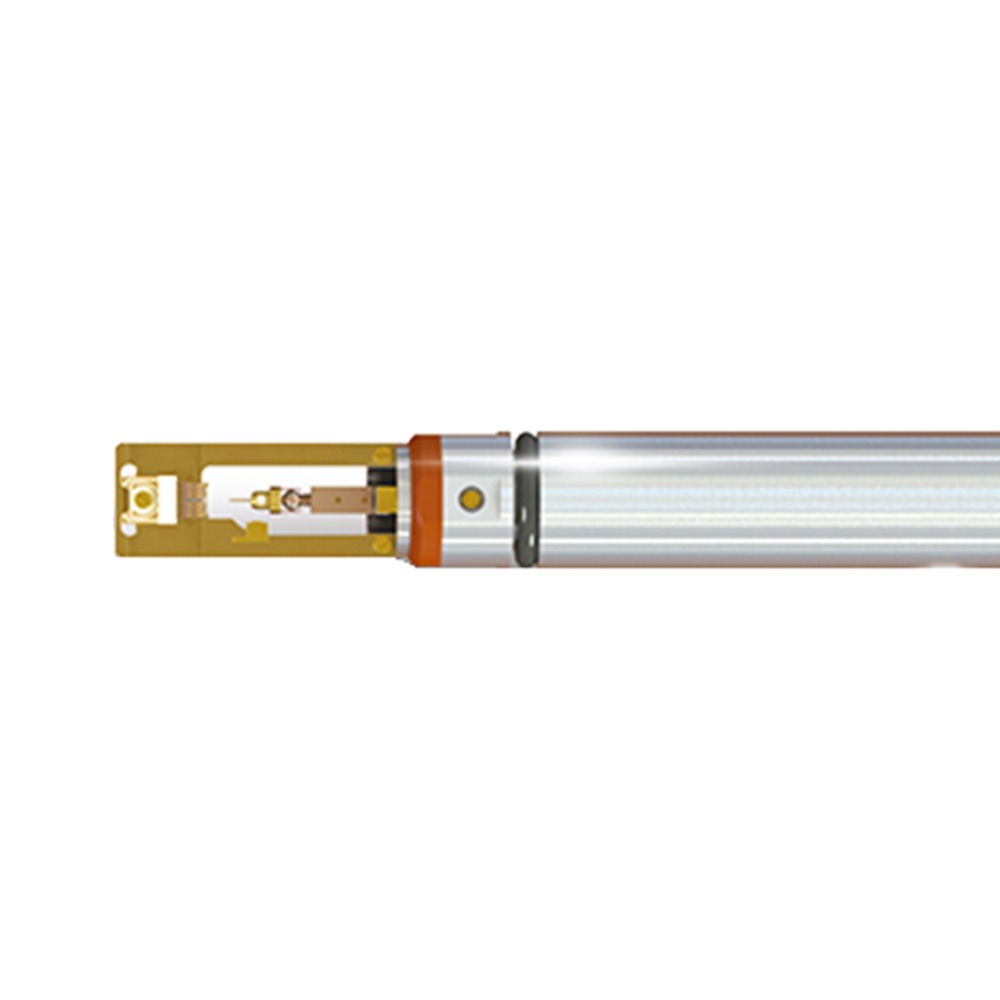
The patented technology (Patent type: Utility model (Electron microscope in-situ sample holder with high-resolution multi-dimensional manipulation and electrical measurement) Patent No.: 202020944865.4) “claw-ball” structure of the probe rod is recognised as a durable and robust probe rod due to its unique structural design.
The equipment’s tip preparation system allows for the cost-effective preparation of tip consumables. The “claw-ball” micromotion structure has been realised in modular mass production with low maintenance cost.