Home » Link Gulf – Main Store Page » Scanning Electron Microscopy » Automatic Stylus Profiler JS2000C
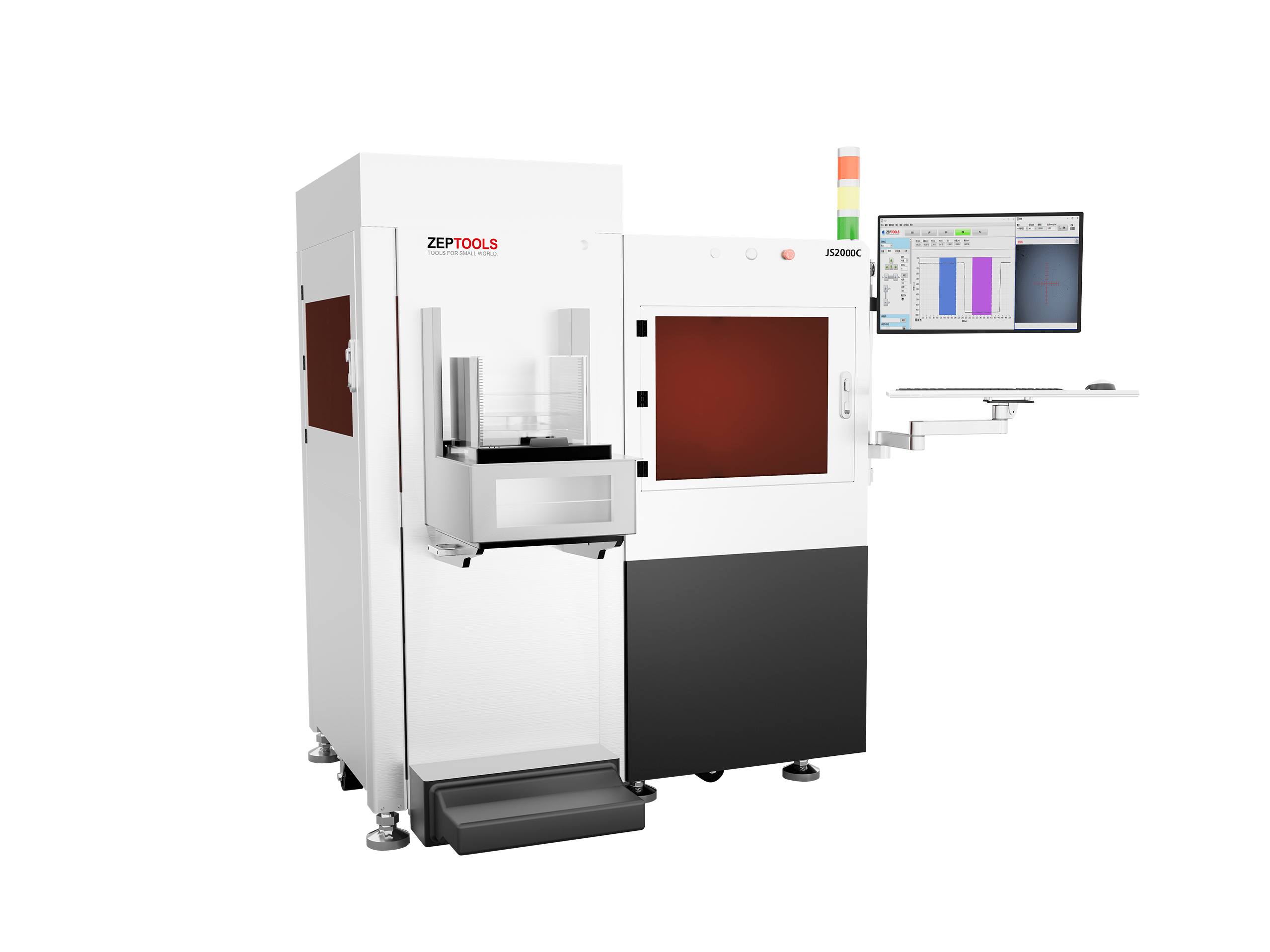
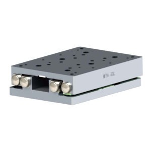
Automatic Stylus Profiler JS2000C
Domestic automatic stylus profiler JS2000C, with high accuracy and high decomposition ability, with a one-piece granite structure, provides stable and reliable repeatability measurement.
JS2000C provides two colour cameras to image the sample and the tip of the needle at the same time, which can observe the sample area without aberration, and it is convenient to locate the feature area. Meanwhile, when scanning with the probe, the scanning area can be observed in real time.
Features
Accurate measurement, rich functionality, all-in-one integration, modular design, convenient after-sales service, and excellent cost performance.
Applications
Request a Quote
Prices shown are for the United Arab Emirates only and exclude VAT @ 5% Local Rate (Unless Otherwise Stated).
Other countries may incur additional import duties.
Please Contact Us for further details and pricing for your country or location.
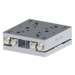
Automatic Stylus Profiler JS2000C
Domestic automatic stylus profiler JS2000C, with high accuracy and high decomposition ability, with a one-piece granite structure, provides stable and reliable repeatability measurement.
JS2000C provides two colour cameras to image the sample and the tip of the needle at the same time, which can observe the sample area without aberration, and it is convenient to locate the feature area. Meanwhile, when scanning with the probe, the scanning area can be observed in real time.
Accurate measurement, rich functionality, all-in-one integration, modular design, convenient after-sales service, and excellent cost performance.
Request a Quote
Request a Quote
Request a Quote
Request a Quote
Request a Quote